Crystal oscillator frequency doubling interference (high-order harmonic radiation) poses a significant challenge in electromagnetic compatibility (EMC) design, typically manifesting as excessive radiation at the 5th and 7th harmonics of the 25MHz fundamental frequency (e.g., 125MHz, 175MHz). This phenomenon arises from the square wave signals emitted by crystal oscillators, which contain abundant harmonic components. When combined with improper PCB layout, these signals can transform into highly efficient radiation antennas.
The following aspects are recommended to solve the problem: source inhibition, path cutting, and circuit optimization.
1. Optimize PCB Layout and Wiring (Most Cost-Effective and Widely Used)
This is the first step in addressing radiation issues, and in many cases, simply modifying the board can resolve most problems.
Guard Ring: A GND network is applied around the signal lines of the crystal oscillator (particularly the output terminals), with a row of ground vias (Via) drilled around it. This effectively blocks signal radiation paths, creating a protective barrier for the signal lines.
Shorten the length of the trace: the trace from the crystal oscillator output pin to the main chip must be as short and straight as possible to avoid the trace length forming antenna effect radiation noise.
Bottom excavation and paving:
① The PCB layer directly beneath the surface-mount crystal oscillator (particularly the top layer) must not accommodate additional signal traces. It is recommended to either perform a controlled 'cutout' on the reference layer (e.g., ground plane) beneath the oscillator, or ensure a fully functional ground plane is maintained as the return path.
② If the crystal oscillator housing requires grounding, ensure the grounding pin is connected to the ground plane with low impedance.
Keep away from sensitive signals: The crystal oscillator trace should be positioned away from high-speed or sensitive signal lines such as USB, Ethernet ports, and RF to prevent crosstalk.
2. Addition of Absorption and Filtering Circuit (Hardware Modification)
If the board cannot be modified in time, or if further radiation reduction is required, components can be added to the circuit.
Series resistor/magnetic bead: A small resistor (0Ω to 33Ω) connected in series with the crystal oscillator's output pin (placed near the oscillator) can suppress high-frequency harmonic oscillations, reduce signal edge overshoot and ringing, thereby lowering EMI.
RC absorption circuit: A RC low-pass filter network (e.g., a series 10-100Ω resistor and a parallel 10-100pF capacitor to ground) is added to the input/output pin of the crystal oscillator, which can absorb resonant energy in specific frequency bands.
Power filtering: A decoupling capacitor (typically 0.1μF ceramic) must be placed at the power pin (VCC) of the crystal oscillator, positioned as close to the power pin as possible. This helps filter out high-frequency noise from the power line and prevents radiation of noise through the power line.
3. Replacement of Crystal Oscillator Type (Source Control)
If the circuit board is finalized and the traces cannot be modified, replacing the crystal oscillator model is the most effective solution.
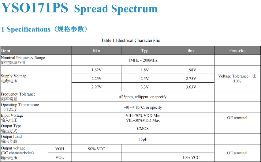
Spread Spectrum Oscillator: This type of oscillator disperses energy originally concentrated at a single frequency point into a wide frequency band through fine frequency modulation, significantly reducing peak radiation power (typically by over 10dB).

Active crystal oscillator (with enable pin): Compared to passive crystal oscillators, active crystals deliver superior waveform quality (typically square waves or clipped sine waves), exhibit stronger driving capability, show minimal sensitivity to peripheral circuit interference, and generally outperform passive crystals in radiation characteristics.
Selecting low-EMI models: When purchasing, focus on the phase noise and harmonic suppression performance of the crystal oscillator. Oscillators with lower phase noise typically exhibit reduced harmonic energy.
4. Shielding and Isolation (Physical Measures)
As the ultimate ultimate move, it's perfect for scenarios with intense radiation.
Shielding enclosure: Use a metal shielding enclosure (Can) to fully enclose the crystal oscillator and its circuitry, ensuring a low-impedance connection between the enclosure and the PCB ground plane through via holes.
Single-point grounding: For passive crystal oscillators, ensure proper grounding design for both pins to prevent noise introduction from ground loops.
In summary, I recommend first checking whether the ground plane has been applied around the crystal oscillator on the PCB. This is the most overlooked yet effective method. If that doesn't work, try adding a small resistor in series at the output.