The output waveform of a crystal oscillator (XO) is a technical parameter as important as the package size. These output waveforms can be broadly classified into two types: sine wave and square wave.
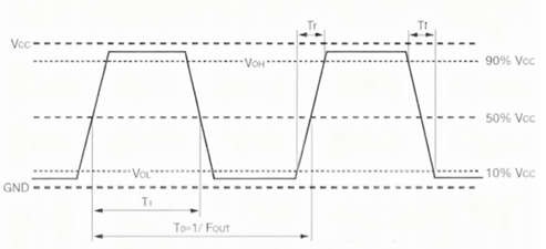
When observing the oscillator waveform on an oscilloscope, it often appears as a sine wave, which is due to insufficient oscilloscope bandwidth. For example, with a 20MHz active crystal oscillator, if measured with a 40MHz or 60MHz oscilloscope, it will display a sine wave. This is because the Fourier decomposition of a square wave is a superposition of the fundamental frequency and odd harmonics. With insufficient bandwidth, only the fundamental frequency of 20MHz and the 60MHz harmonic remain, thus displaying a sine wave. Perfect reproduction of a square wave requires at least 10 times the bandwidth; 5 times the bandwidth is only barely sufficient, requiring at least a 100MHz oscilloscope.
In digital communication systems, crystal oscillators with square wave output are generally used to match the load driven by the system. Common output types for these square waves include TTL and CMOS, as well as LVPECL and LVDS. Key parameters include output level, duty cycle, rise/fall time, and drive capability.
(1) TTL Output
TTL is a Transistor-Transistor Logic circuit, characterized by fast transmission delay time and high power consumption. It is a current-controlled device.
(2) CMOS Output
CMOS output is the most common type, a voltage-controlled form used to drive logic level inputs.
CMOS output has slower transmission delay time and lower power consumption, offering a larger noise margin compared to TTL, and its input impedance is much greater than that of TTL.
(3) LVPECL Output
LVPECL stands for Low-Voltage Positive Emitter-Coupled Logic. ECL circuits are fast, have strong driving capabilities, and low noise, easily achieving applications in the hundreds of MHz range. However, they consume a lot of power and require a negative power supply. To simplify the power supply, PECL (ECL structure, using positive voltage power supply) and LVPECL output modes were developed.
(4) LVDS Output
LVDS (Low-Voltage Differential Signaling) uses differential pair input and output, with an internal 3.5-4mA constant current source that changes direction and voltage level on the differential lines to represent "1" and "0".
It is converted to a ±350mV differential level through an external 100-ohm matching resistor (connected in parallel on the differential lines near the receiving end). LVDS usage notes: It can reach over 600MHz, requiring high-quality PCBs, and the differential lines must be strictly equal in length, with the difference ideally not exceeding 10 mil (0.25 mm); the 100-ohm resistor should be no more than 500 mil from the receiving end, preferably within 300 mil.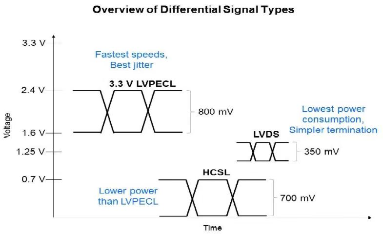
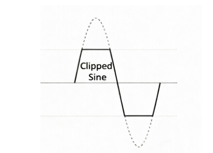
(5) Sine Wave Output Mode
Sine wave output is mainly used in circuits with special requirements for EMI and frequency interference, such as driving RF components, mixers, or other devices with a 50Ω input impedance. In this case, the output power generated by the oscillator is typically between 0dBm and +13dBm (1mW to 20mW), although higher power output is possible if needed.
There is also a special clipped sine wave, which has significantly fewer harmonic components compared to a square wave, but has weaker driving capability. With a 10K//10PF load, the Vp-p is 0.8Vmin.