1. Reference Frequency:
The oscillation frequency of the crystal oscillator under ideal conditions.
2. Operating Voltage:
Crystal oscillators require a certain external power supply voltage to operate. The noise on the clock signal output by the crystal oscillator is closely related to the power supply; therefore, the crystal oscillator's datasheet specifies certain requirements for power supply quality.
3. Output Level:
Compared to crystals, the most prominent feature of crystal oscillators is that they directly output a clock signal as soon as power is applied. The clock signal levels are diverse, supporting levels including: TTL, CMOS, HCMOS, LVCOMS, LVPECL, LVDS, etc. When selecting a crystal oscillator, choose one that matches the required clock signal level.
4. Operating Temperature Range:
Select the appropriate operating temperature range based on the environmental temperature requirements.
5. Frequency Accuracy:
Different frequency accuracies can be selected for different operating temperature ranges. Taking ±15ppm, -20~70℃ as an example, it means that within the temperature range of -20~70℃, the deviation of the crystal oscillator's output frequency from the reference frequency will not exceed 15ppm. This parameter is an important parameter of the crystal oscillator and includes frequency deviations caused by factors such as temperature changes, power supply voltage fluctuations, and load changes.
6. Aging Rate:
The relationship between frequency accuracy and time when the crystal oscillator frequency is measured under constant external conditions.
7. Startup Time:
The time required from power-on until the deviation of the crystal oscillator's output frequency reaches the specified frequency accuracy.
8. Clock Jitter:
Period jitter (JPER) is the time difference between the measured period and the ideal period. Due to its random distribution characteristics, it can be described by peak-to-peak or root mean square (RMS) values. First, define the clock rising edge at threshold VTH as TPER(n) in the time domain, where n is a time domain system, as shown in the figure. JPER is expressed as:
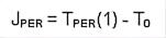
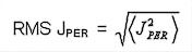
Where T0 is the ideal clock period. Since the clock frequency is fixed, the mean of the random jitter JPER should be zero, and the RMS of JPER can be expressed as:
The figure below shows the period jitter measurement.
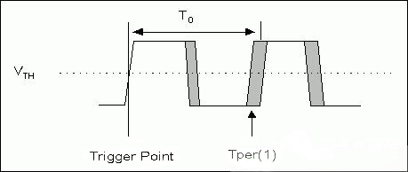
Using the edge trigger and persistence function of an oscilloscope, the signal jitter can be roughly measured. However, measurements using this method are not practically meaningful. (1) As the measurement time increases, the measured jitter value will continuously increase, meaning that this measurement method cannot yield a definitive jitter value; (2) Even if a definitive jitter value could be obtained, such a value would have no practical guidance for circuit design and could only provide a rough estimate of the jitter characteristics of the crystal oscillator used.
9. Phase Noise:
In the frequency domain, data offset is defined by phase noise. For a clock signal with frequency f0, if the signal contains no jitter, all the signal power should be concentrated at the frequency point f0. However, since all signals have jitter, some of which is random and some deterministic, distributed over a considerably wide frequency band, the presence of jitter will cause the signal power to be spread across these frequency bands. The phase noise of a signal is the power component of the signal at a specific frequency. The curve formed by connecting these components is the phase noise curve. Phase noise is usually defined as the dBc/Hz value at a given offset, where dBc is the ratio of the power at that frequency to the total power in dB. For example, the phase noise of an oscillator at a certain offset frequency is defined as the ratio of the signal power within a 1Hz bandwidth at that frequency to the total signal power, i.e., the ratio of the area within the 1Hz range at frequency fm to the total area under the entire noise frequency spectrum.
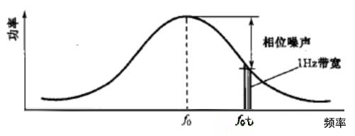
Signal Phase Noise Curve Diagram
From the phase noise curve diagram, it can be seen that most of the jitter is concentrated near the frequency f0, and the further away from f0 the frequency band is, the smaller the jitter energy.
The following example illustrates the requirements for clock input:
RMS JPER (12kHz~20MHz): 0.5ps
Phase Noise (10~100kHz): -120dBc/Hz
These are actually two requirements: one requires that the root mean square jitter in the frequency band of 12kHz~20MHz should not exceed 0.5ps; the other requires that the power spectral density at any frequency point in the frequency band of 10~100kHz should not exceed -120dBc/Hz.