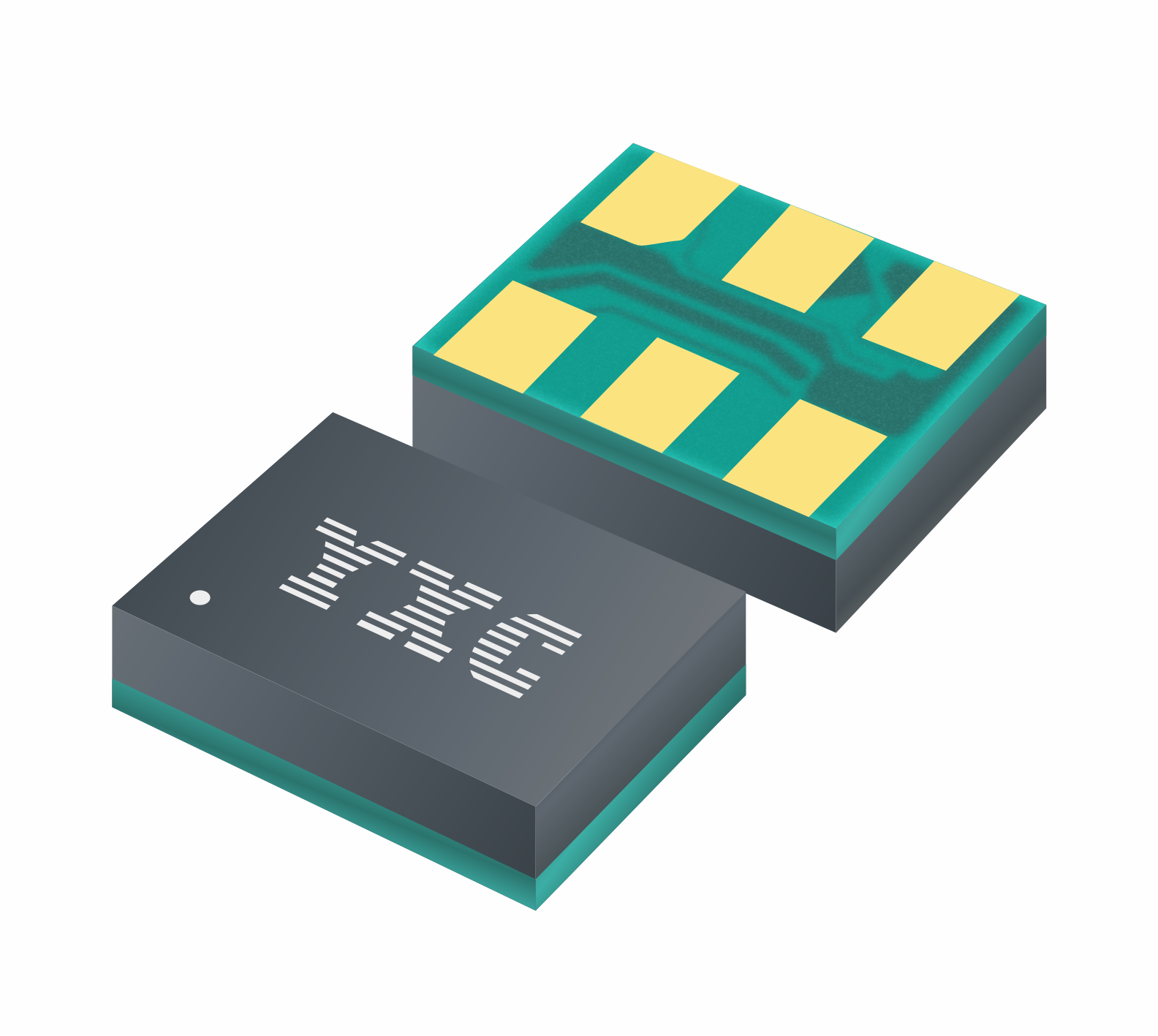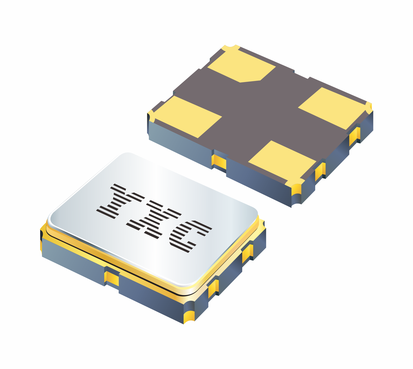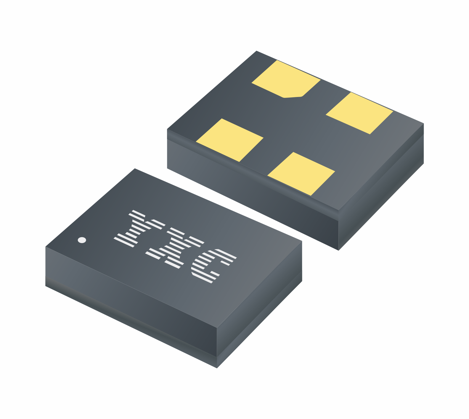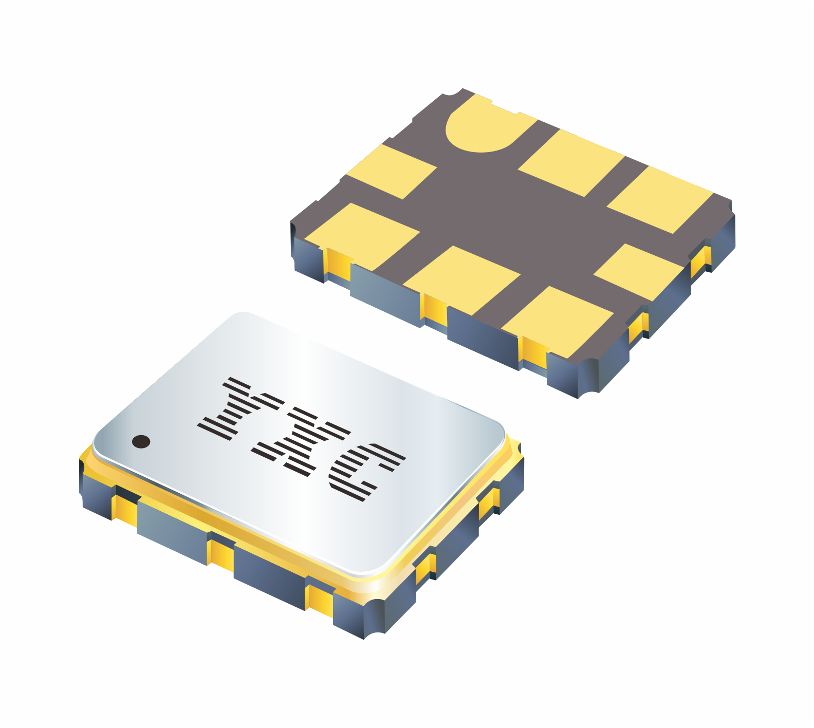
SG-8018CE SG-8018CB SG-8018CA
ROHS STATUS: Compliant
Applications: Cellphone, Tablet, Health and Wellness Monitors Fitness watches, Sports Video Cams
|
Item
|
Symbol
|
Specifications
|
Conditions/Remarks
|
|||||||||||||
|
Supply voltage
|
VCC
|
1.80 V Typ.
|
2.50 V Typ.
|
3.30 V Typ.
|
||||||||||||
|
1.62 to 1.98V
|
1.98 to 2.20V
|
2.20 to 2.80V
|
2.70 to 3.63 V
|
|||||||||||||
|
Output frequency range
|
f0
|
0.67 MHz to 170 MHz
|
||||||||||||||
|
Storage temperature
|
T_stg
|
-40°C to +125°C
|
Storage as single product.
|
|||||||||||||
|
Operating temperature
|
T_use
|
H: -40°C to +105°C
|
||||||||||||||
|
Frequency tolerance *1
|
f_tol
|
J: ±50 × 10-6
|
T_use= -40°C to +105°C
|
|||||||||||||
|
Current consumption
|
ICC
|
3.2mA Max.
|
3.3mA Max.
|
3.4mA Max.
|
3.5mA Max.
|
T_use=+105°C
|
No load
f0 = 20 MHz |
|||||||||
|
2.7mA Typ.
|
2.9mA Typ.
|
3.0mA Typ.
|
T_use=+25°C
|
|||||||||||||
|
5.5mA Max.
|
5.8mA Max.
|
6.7mA Max.
|
8.1mA Max.
|
T_use=+105°C
|
No load
f0 = 170 MHz |
|||||||||||
|
4.7mA Typ.
|
5.7mA Typ.
|
6.8mA Typ.
|
T_use=+25°C
|
|||||||||||||
|
Output disable current
|
I_dis
|
3.2mA Max.
|
3.2mA Max.
|
3.3mA Max.
|
3.5mA Max.
|
OE=GND , f0 = 170 MHz
|
||||||||||
|
Standby current
|
I_std
|
0.9μA Max.
|
1.0μA Max.
|
1.5μA Max.
|
2.5μA Max.
|
T_use=+105°C
|
ST = GND
|
|||||||||
|
0.3μA Typ.
|
0.4μA Typ.
|
0.5μA Typ.
|
1.1μA Typ.
|
T_use= +25°C
|
||||||||||||
|
Symmetry
|
SYM
|
45% to 55%
|
50% VCC Level
|
|||||||||||||
|
Output voltage
(DC characteristics) |
VOH | 90% VCC Min. | [mA] | |||||||||||||
| tr / tf | VCC | A | B | C | D | |||||||||||
| Default (f0>40MHz) Fast |
IOH | -2.5 | -3.5 | -4.0 | -5.0 | |||||||||||
| IOL | 2.5 | 3.5 | 4.0 | 5.0 | ||||||||||||
| Default (f0≦40MHz) |
IOH | -1.5 | -2.0 | -2.5 | -3.0 | |||||||||||
| VOL | 10% VCC Max. | IOL | 1.5 | 2.0 | 2.5 | 3.0 | ||||||||||
| Slow | IOH | -1.0 | -1.5 | -2.0 | -2.5 | |||||||||||
| IOL | 1.0 | 1.5 | 2.0 | 2.5 | ||||||||||||
| A: 1.62 to 1.98 V , B: 1.98 to 2.20 V C: 2.20 to 2.80 V , D: 2.70 to 3.63 V |
||||||||||||||||
| Output load condition | L_CMOS | 15pF Max. | ||||||||||||||
| Input voltage | VIH | 70% VCC Min. | OE or ST | |||||||||||||
| VIL | 30% VCC Max. | |||||||||||||||
| Rise and Fall time | Default | tr / tf | 3.0 ns Max. | f0 > 40MHz | 20% VCC to 80% VCC L_CMOS=15pF |
|||||||||||
| 6.0 ns Max. | f0 ≦ 40MHz | |||||||||||||||
| Fast | 3.0 ns Max. | f0=0.67to170MHz | ||||||||||||||
| Slow | 10.0 ns Max. | f0=0.67to20MHz | ||||||||||||||
| Disable Time | t_stp | 1 μs Max. | Measured from the time OE or ST pin crosses 30 % VCC |
|||||||||||||
| Enable Time | t_sta | 1 μs Max. | Measured from the time OE pin crosses 70 % VCC |
|||||||||||||
| Resume Time | t_res | 3 ms Max. | Measured from the time ST pin crosses 70 % VCC |
|||||||||||||
| Start-up time | t_str | 3 ms Max. | Measured from the time VCC reaches its rated minimum value, 1.62 V |
|||||||||||||
| Frequency aging | f_aging | This is included in frequency tolerance specification | +25°C, 10 years | |||||||||||||
| Pin | Name | I/O type | Function | |
| 1 | OE | Input | Output enable | High: Specified frequency output from OUT pin Low: Out pin is low (weak pull down), only output driver is disabled. |
| ST | Input | Standby | High: Specified frequency output from OUT pin Low: Out pin is low (weak pull down) Device goes to standby mode. Supply current reduces to the least as I_std. |
|
| 2 | GND | Power | Ground | |
| 3 | OUT | Output | Clock output | |
| 4 | VCC | Power | Power supply | |
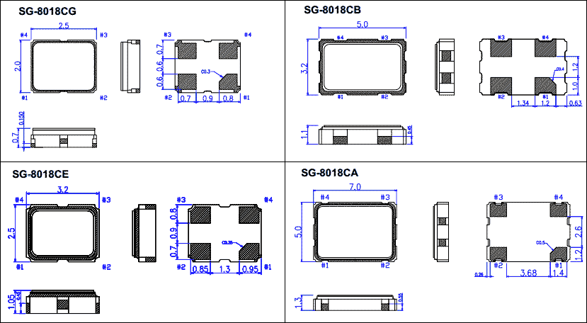
(Unit: mm)
To maintain stable operation, provide a 0.1µF by-pass capacitor at a location as near as possible to the power source terminal of the crystal product
(between VCC - GND).
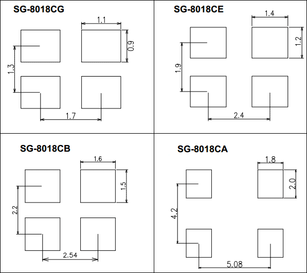
Footprint (Recommended)
Voltage : 1.62V~3.63V
Frequency : 0.67MHz-170MHz
Dimension : 2.5 x 2.0 mm 3.2 x 2.5 mm 5.0 x 3.2 mm 7.0 x 5.0 mm
Operating Temp :
Frequency Tolerance : ±50ppm
Output : CMOS