Clock Chip
* The SYKB23F10(G) is an 11-output (10 differential outputs + 1 single-ended output) ultra-low additive jitter differential clock buffer.
* It supports three input reference clocks (two differential/single-ended clock inputs supporting up to 3.1 GHz, and one crystal input).
* The system distributes the selected reference clock to two output groups, providing ten differential clock outputs (five per output group, supporting LVPECL/LVDS/LP_HCSL) and one LVCMOS clock output. The maximum operating frequency of the differential clocks is up to 3.1 GHz.
* It is designed for high-frequency clock/data distribution and multi-stage conversion in complex systems. Models with the "G" suffix also support glitch-free switching.
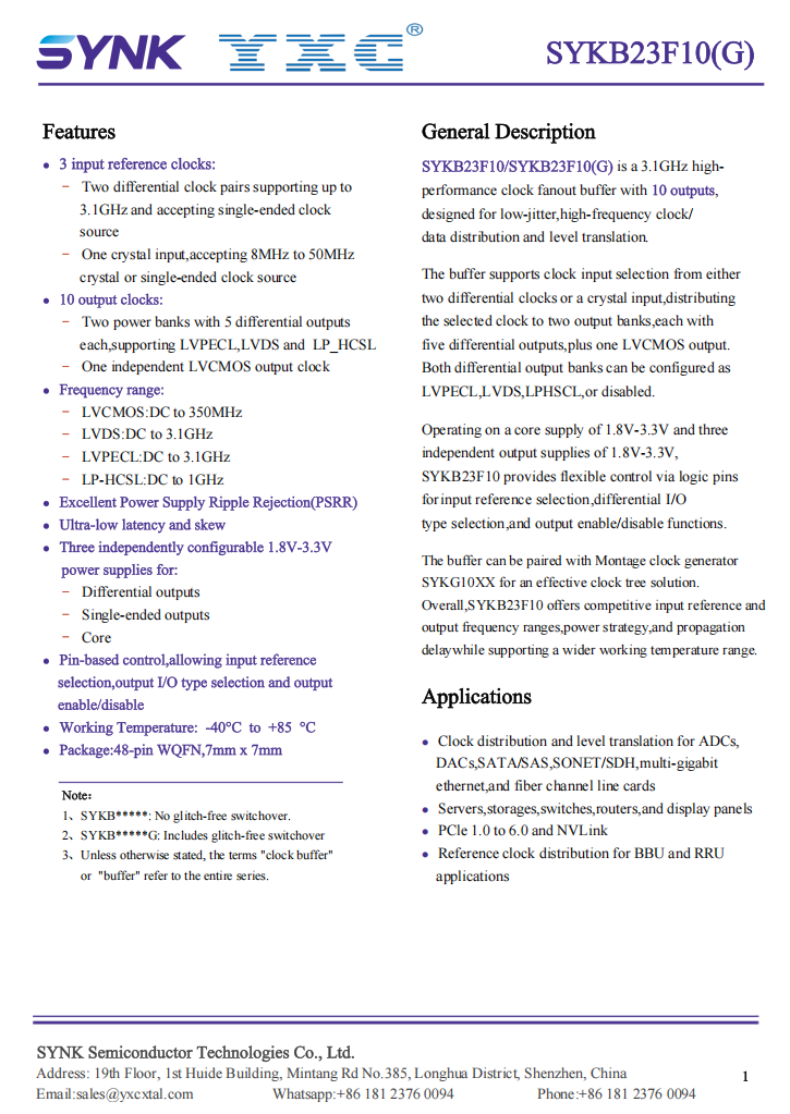
Voltage : 1.8V~3.3V
Frequency :
Dimension :
Operating Temp :
Frequency Tolerance :
Output :
Series : SYKB23F10G
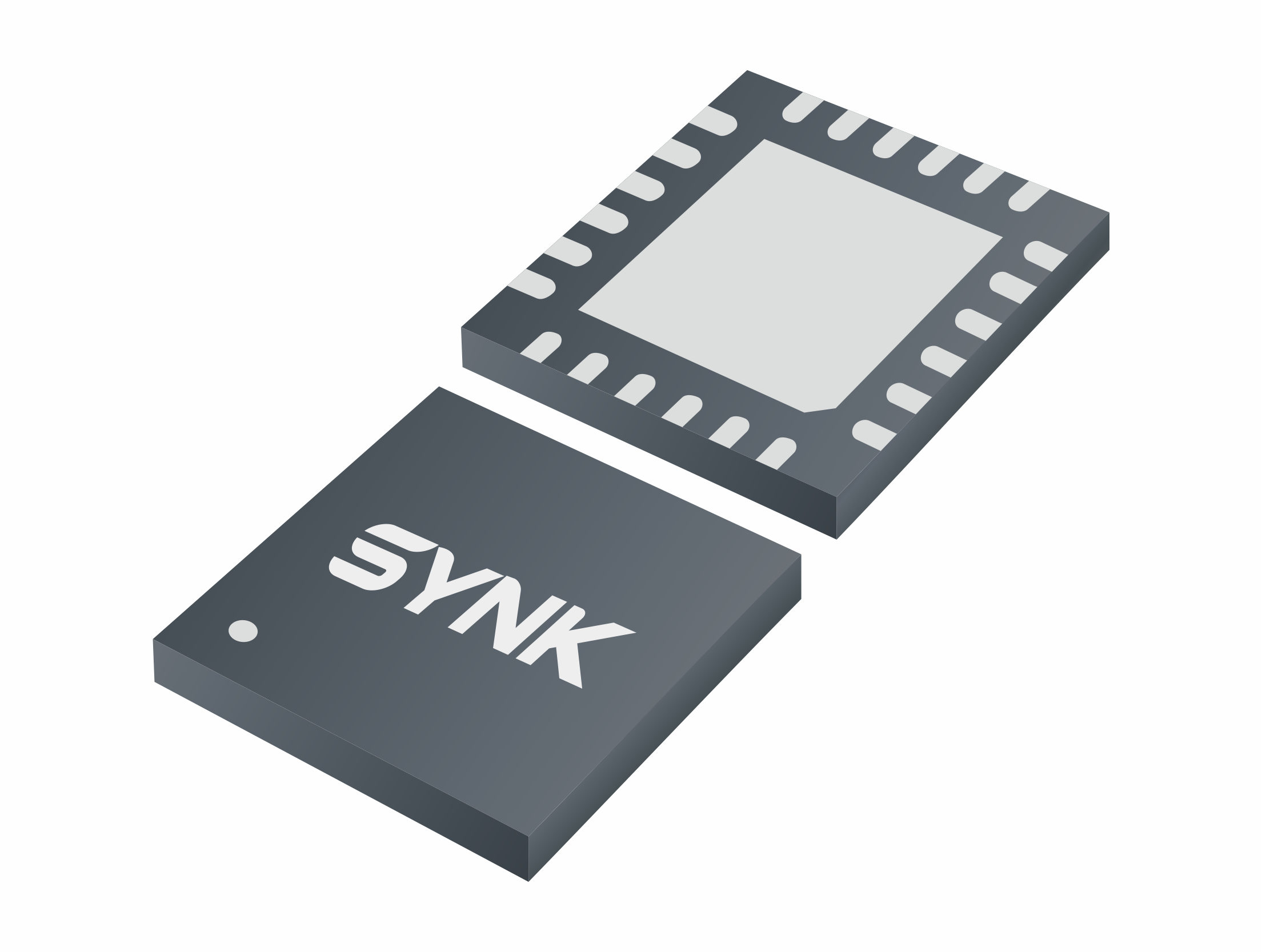
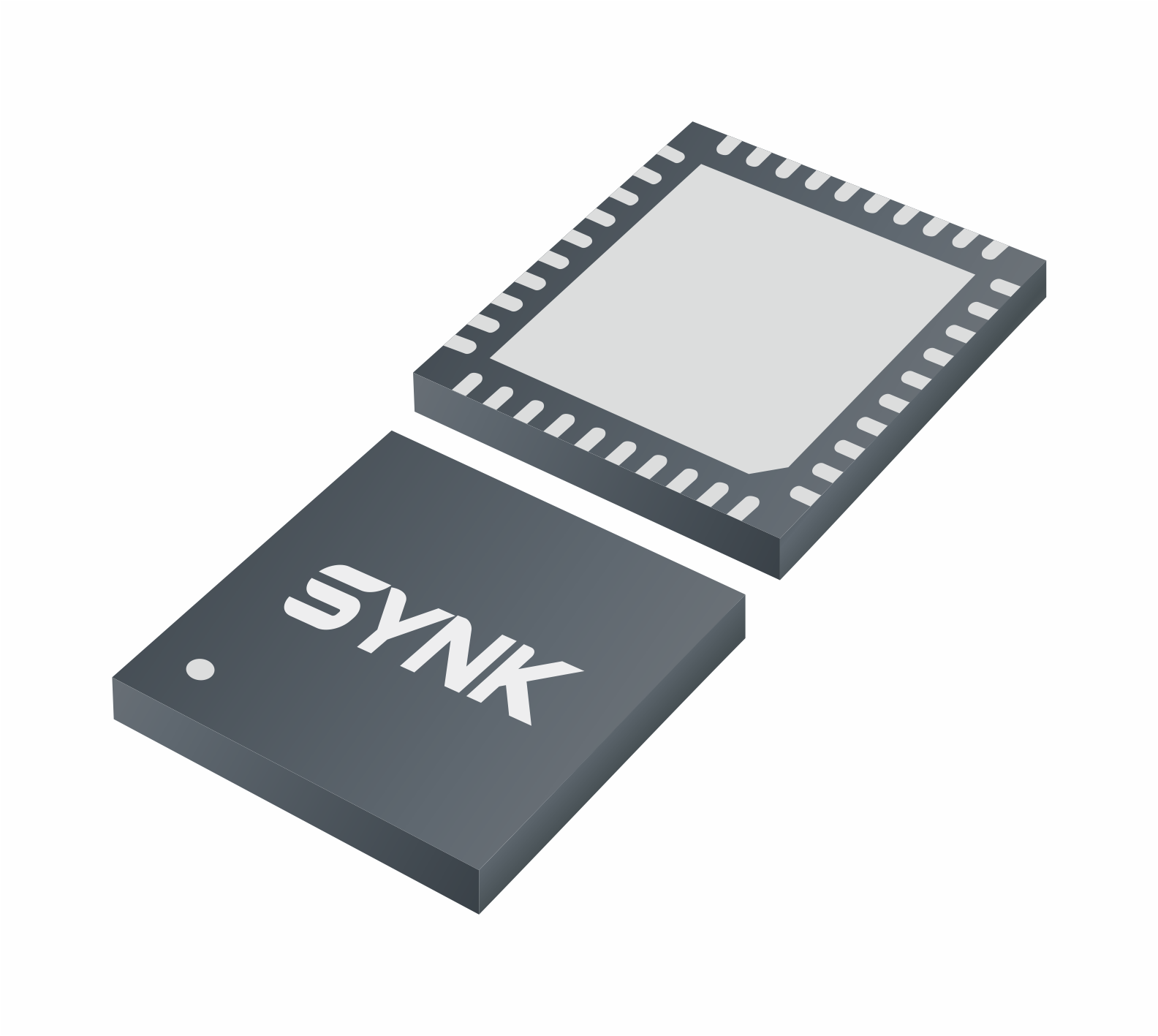
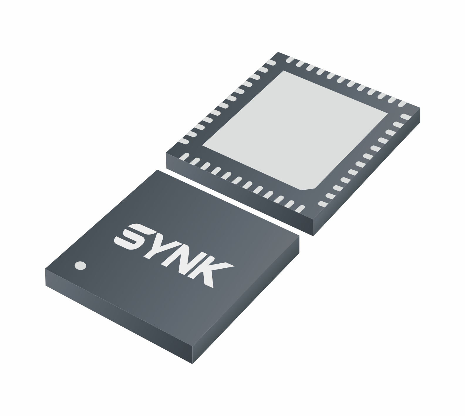
Package : 48-pin WQFN
Output Freq : LVCMOS:350MHz LVDS/PECL:3.1GHz HCSL:1GHz
Output Type : LVPECL LVDS LP-HCSL LVCMOS
Output Qty : 10 Diff+1 SE
Input Type : 3Inputs(2Diff/1Xtal)
Temp : -40~+85℃
Jitter : 34fs (156.25MHz) 10fs (PCIe Gen5)